- 您现在的位置:买卖IC网 > Sheet目录369 > W948D2FBJX5E (Winbond Electronics)IC LPDDR SDRAM 256MBIT 90VFBGA
�� �
�
�W948D6FB� /� W948D2FB�
�256Mb� Mobile� LPDDR�
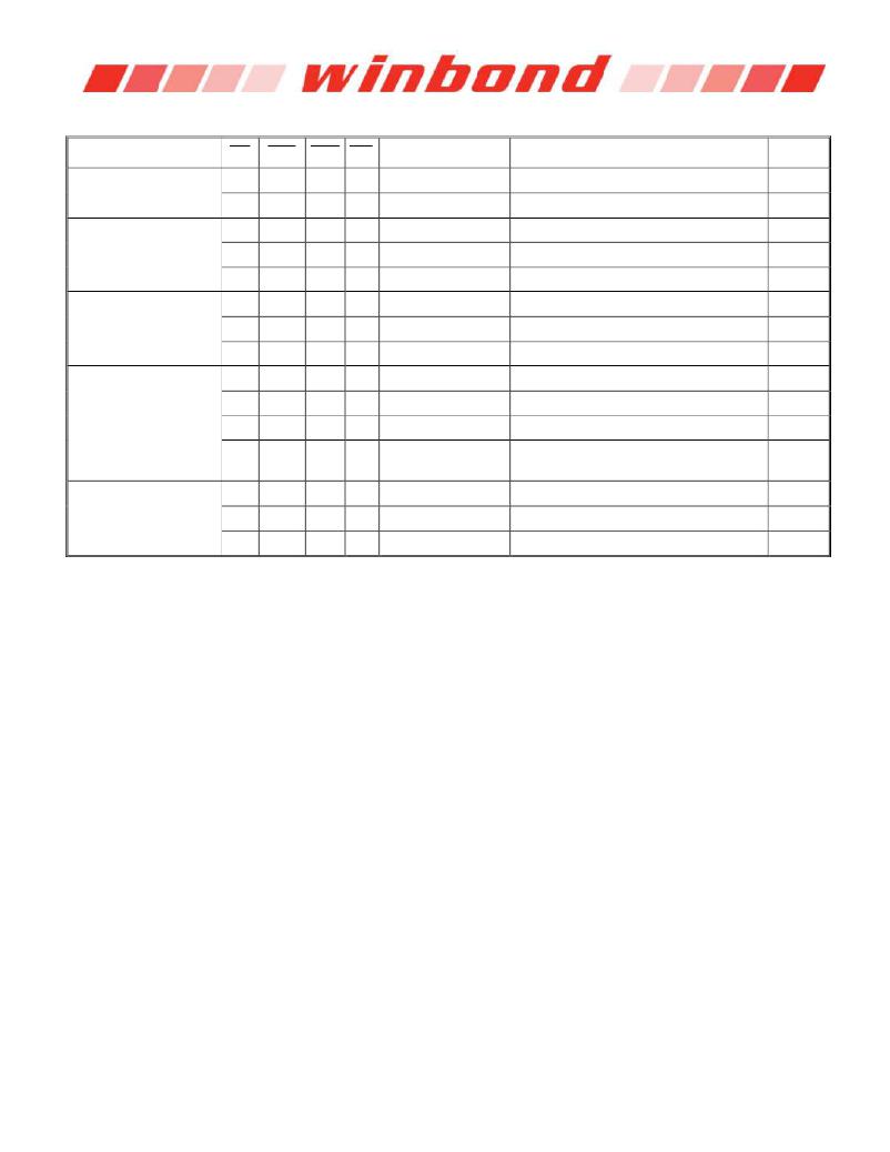
�6.11.5� Truth� Table� -� Current� State� BANKn� -� Command� to� BANKn�
�CURRENT� STATE�
�CS�
�RAS� CAS� WE�
�COMMAND�
�ACTION�
�NOTES�
�Any�
�H�
�L�
�L�
�X�
�H�
�L�
�X�
�H�
�H�
�X�
�H�
�H�
�DESELECT�
�No� Operation�
�ACTIVE�
�NOP� or� Continue� previous� operation�
�NOP� or� Continue� previous� operation�
�Select� and� activate� row�
�Idle�
�Row� Active�
�Read� (Auto� precharge�
�Disabled)�
�Write� (Auto� precharge�
�Disabled)�
�L�
�L�
�L�
�L�
�L�
�L�
�L�
�L�
�L�
�L�
�L�
�L�
�L�
�L�
�H�
�H�
�L�
�H�
�H�
�L�
�H�
�H�
�H�
�L�
�L�
�L�
�L�
�L�
�H�
�L�
�L�
�H�
�H�
�L�
�L�
�H�
�H�
�L�
�H�
�L�
�L�
�H�
�L�
�L�
�L�
�H�
�L�
�L�
�AUTO� REFRESH�
�MRS�
�READ�
�WRITE�
�PRECHARGE�
�READ�
�WRITE�
�PRECHARGE�
�BURST�
�TERMINATE�
�READ�
�WRITE�
�PRECHARGE�
�Auto� refresh�
�Mode� register� set�
�Select� column� &� start� read� burst�
�Select� column� &� start� write� burst�
�Deactivate� row� in� bank� (or� banks)�
�Select� column� &� start� new� read� burst�
�Select� column� &� start� write� burst�
�Truncate� read� burst,� start� precharge�
�Burst� terminate�
�Select� column� &� start� read� burst�
�Select column & start new write burst�
�Truncate write burst & start precharge�
�10�
�10�
�4�
�5,� 6�
�5,� 6,� 13�
�11�
�5,� 6,� 12�
�5,� 6�
�12�
�Notes:�
�1.�
�2.�
�3.�
�4.�
�5.�
�6.�
�7.�
�8.�
�9.�
�The� table� applies� when� both� CKEn-1� and� CKEn� are� HIGH,� and� after� tXSR� or� tXP� has� been� met� if� the� previous� state� was�
�Self� Refresh� or� Power� Down.�
�DESELECT� and� NOP� are� functionally� interchangeable.�
�All� states� and� sequences� not� shown� are� illegal� or� reserved.�
�This� command� may� or� may� not� be� bank� specific.� If� all� banks� are� being� precharged,� they� must� be� in� a� valid� state� for�
�precharging.�
�A� command� other� than� NOP� should� not� be� issued� to� the� same� bank� while� a� READ� or� WRITE� burst� with� Auto� Precharge� is�
�enabled.�
�The� new� Read� or� Write� command� could� be� Auto� Prechrge� enabled� or� Auto� Precharge� disabled.�
�Current� State� Definitions:�
�Idle:� The� bank� has� been� precharged,� and� tRP� has� been� met.�
�Row� Active:� A� row� in� the� bank� has� been� activated,� and� tRCD� has� been� met.� No� data� bursts/accesses� and� no� register�
�accesses� are� in� progress.�
�Read:� A� READ� burst� has� been� initiated,� with� Auto� Precharge� disabled,� and� has� not� yet� terminated� or� been� terminated.�
�Write:� A� WRITE� burst� has� been� initiated,� with� Auto� Precharge� disabled,� and� has� not� yet� terminated� or� been� terminated.�
�The� following� states� must� not� be� interrupted� by� a� command� issued� to� the� same� bank.� DESEDECT� or� NOP� commands� or�
�allowable� commands� to� the� other� bank� should� be� issued� on� any� clock� edge� occurring� during� these� states.� Allowable�
�commands� to� the� other� bank� are� determined� by� its� current� state� and� this� table,� and� according� to� next� table.�
�Precharging:� Starts� with� the� registration� of� a� PRECHARGE� command� and� ends� when� tRP� is� met.� Once� tRP� is� met,� the�
�bank� will� be� in� the� idle� state.�
�Row� Activating:� Starts� with� registration� of� an� ACTIVE� command� and� ends� when� tRCD� is� met.� Once� tRCD� is� met,� the� bank�
�will� be� in� the� ?row� active?� state.�
�Read� with� AP� Enabled:� Starts� with� the� registration� of� the� READ� command� with� Auto� Precharge� enabled� and� ends� when� tRP�
�has� been� met.� Once� tRP� has� been� met,� the� bank� will� be� in� the� idle� state.�
�Write� with� AP� Enabled:� Starts� with� registration� of� a� WRITE� command� with� Auto� Precharge� enabled� and� ends� when� tRP� has�
�been� met.� Once� tRP� is� met,� the� bank� will� be� in� the� idle� state.�
�The� following� states� must� not� be� interrupted� by� any� executable� command;� DESEDECT� or� NOP� commands� must� be� applied�
�to� each� positive� clock� edge� during� these� states.�
�Refreshing:� Starts� with� registration� of� an� AUTO� REFRESH� command� and� ends� when� tRFC� is� met.� Once� tRFC� is� met,� the�
�LPDDR� SDRAM� will� be� in� an� ?all� banks� idle?� state.�
�Publication� Release� Date� :� Oct,� 15,� 2012�
�-� 22� -�
�Revision� :� A01-004�
�发布紧急采购,3分钟左右您将得到回复。
相关PDF资料
W949D2CBJX5E
IC LPDDR SDRAM 512MBIT 90VFBGA
W971GG6JB25I
IC DDR2 SDRAM 1GBIT 84WBGA
W971GG8JB-25
IC DDR2 SDRAM 1GBIT 60WBGA
W9725G6IB-25
IC DDR2-800 SDRAM 256MB 84-WBGA
W9725G6JB25I
IC DDR2 SDRAM 256MBIT 84WBGA
W9725G6KB-25I
IC DDR2 SDRAM 256MBIT 84WBGA
W972GG6JB-3I
IC DDR2 SDRAM 2GBITS 84WBGA
W9751G6IB-25
IC DDR2-800 SDRAM 512MB 84-WBGA
相关代理商/技术参数
W948D2FBJX5ETR
制造商:Winbond Electronics Corp 功能描述:256M MDDR, X32, 200MHZ
W948D2FBJX5I
制造商:Winbond Electronics Corp 功能描述:DRAM Chip DDR SDRAM 256M-Bit 8Mx32 1.8V 90-Pin VFBGA 制造商:Winbond Electronics Corp 功能描述:IC MEMORY
W948D2FBJX5I TR
制造商:Winbond Electronics Corp 功能描述:256M MDDR, X32, 200MHZ, INDUST
W948D2FBJX6E
制造商:Winbond Electronics Corp 功能描述:DRAM Chip DDR SDRAM 256M-Bit 8Mx32 1.8V 90-Pin VFBGA 制造商:Winbond Electronics 功能描述:LOW POWER DRAM 制造商:Winbond Electronics Corp 功能描述:IC MEMORY
W948D2FBJX6ETR
制造商:Winbond Electronics Corp 功能描述:256M MDDR, X32, 166MHZ, 65NM
W948D2FBJX6G
制造商:WINBOND 制造商全称:Winbond 功能描述:256Mb Mobile LPDDR
W948D6FB
制造商:WINBOND 制造商全称:Winbond 功能描述:256Mb Mobile LPDDR
W948D6FBHX5E
功能描述:IC LPDDR SDRAM 256MBIT 60VFBGA RoHS:是 类别:集成电路 (IC) >> 存储器 系列:- 标准包装:1 系列:- 格式 - 存储器:闪存 存储器类型:闪存 - NAND 存储容量:4G(256M x 16) 速度:- 接口:并联 电源电压:2.7 V ~ 3.6 V 工作温度:0°C ~ 70°C 封装/外壳:48-TFSOP(0.724",18.40mm 宽) 供应商设备封装:48-TSOP I 包装:Digi-Reel® 其它名称:557-1461-6